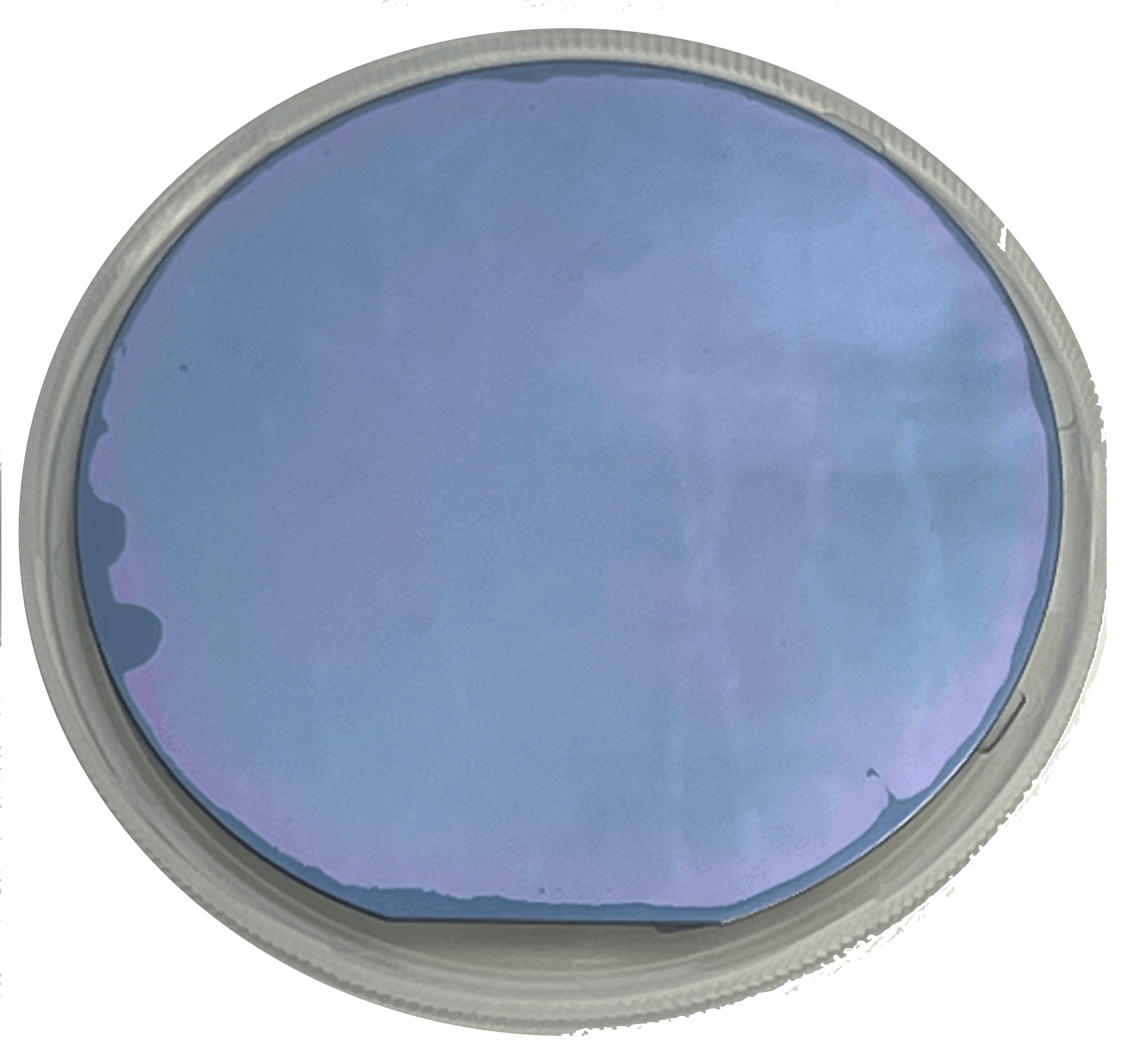
ION SLICED THIN FILMS
Partow’s technology is based on crystal ion slicing of lithium niobate wafers. The process uses ion implantation to weaken the crystal bondage in a lithium niobate wafer. The implanted crystal is then bonded to a handle substrate and a thin layer of lithium niobate is transferred to the handle substrates using crystal ion slicing technique. A final chemical-mechanical polishing step smoothens the surface of the bonded thin film wafer. Currently, the company produces customized photonic thin film platforms using its thin film bonding system and can extend its process to provide more customized bonded platforms based on customer’s needs and application.

Smart cut thin film lithium niobate on silicon product specification
| Part Number | LN-X-600-2000-100-100 | LN-X-xxx-xxx-xx-100 |
|---|---|---|
| Description | X-cut lithium niobate single crystal on silicon dioxide on silicon | |
| Top lithium niobate layer | ||
| Parameter | Standard | Custom Order |
| Orientation | X-cut | X-cut, Y-cut or Z-cut |
| Primary Flat (on LN film) | +z | TBD |
| Secondary Flat (on LN film) | -Y | TBD |
| Lithium Niobate Film Diameter | 100 mm | None |
| Thickness |
600 nm | 300 – 1,000 nm |
| Thickness Uniformity | < 2% | < 1% |
| Surface Roughness | < 1 nm | < 1 nm |
| Defective Area >100micron | < 5% | < 5% |
| Defective Area <100micron | < 1 per inch2 | < 1 per inch2 |
| Intermediate SiO2 layer | ||
| Parameter | Standard | Custom Order |
| Thickness Range | 2,000 nm | 0 nm – 6,000 nm |
| Thickness Uniformity | < 3% | < 3% |
| Silicon Substrate | ||
| Parameter | Standard | Custom Order |
| Substrate Thickness | 0.5 mm | 0.5 – 1 mm |
| Substrate Diameter | 100 mm | 100 |
| Substrate Resistivity | > 5000 ohm-cm | 0 – 20,000 ohm-cm |
