BONDING
Room temperature wafers bonding equipment and service
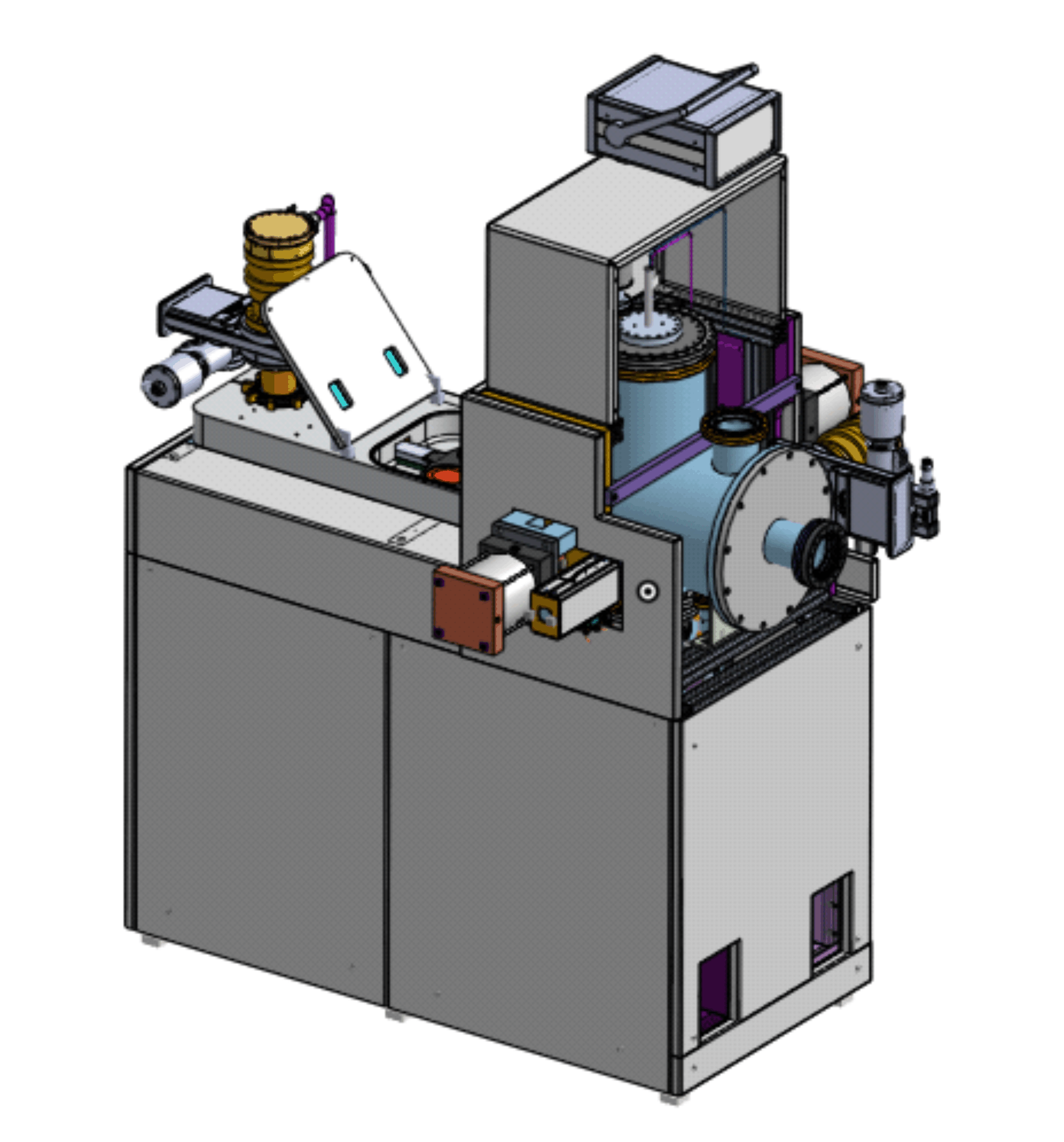
- Home designed plasma assisted UHV vacuum system for wafer bonding
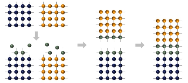
- Surface of wafers are activated using plasma source in the high vacuum chamber
- Wafers are pressed inside the vacuum
- Active atoms on the surface of wafers diffuse and form an atomic diffusion bond
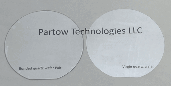
- Bond strength is so high that it is impossible to separate the wafers without breakage
- Materials with different thermal expansion coefficients can bond to each other since no heating is required
- Brittle materials such as InP or GaAs can bond to Silicon or other materials since no high forces are required
- No intermediate layer is required so the bond interface is transparent to light and heat.

Applications
- Transparent optical bonding
- Bonding of photodetector and various optical elements on different substrates
- Wafer level packaging
- MEMS encapsulation and device fabrication
- Functional wafer fabrication such as lithium niobate thin films on Silicon
Features
- No intermediate layers
- No heating is required
- No high force or high pressure is required
- Very strong bond higher than yield strength of many materials is obtained
- Dissimilar wafer bonding up to 4″ wafers


Example Substrates
- GaAs, LiNbO3, Quartz, Silicon, GaN, Germanium, Saphire
- Metal to metal surface bonding
- Oxide to metal bonding
- Semiconductor to semiconductor bonding
- Semiconductor to oxide bonding
- Oxide to oxide bonding
Requirements
| Parameter | Substrate I | Substrate II |
|---|---|---|
| Material | Silicon, Lithium Niobite, Quartz, GaAs, InP | Silicon, Lithium Niobite, Quartz, GaAs, InP |
| Diameter | 25 mm, 100 mm | 25 mm, 100 mm |
| Thickness | 100 µm to 1 mm | 100 µm to 1 mm |
| Surface Roughness | <0.5 nm | <0.5 nm |
